
pcb engineering

PCB design for industrial and embedded electronics

We develop production-ready printed circuit boards: component placement, routing, stack-up, power distribution, interface constraints, DFM and manufacturing data.

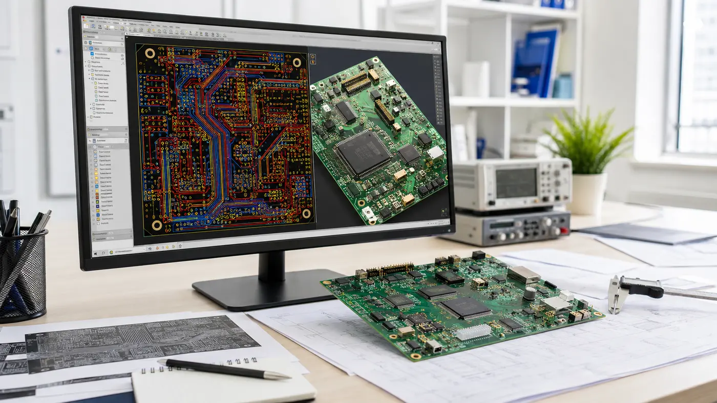
Detailed PCB layout and manufactured industrial electronics board

You can start with a practical problem

You do not need to prepare formal engineering terminology before contacting us. A clear business or equipment problem is enough for an initial technical discussion.

What we do

ReviewSchematics, mechanical envelope, connectors and manufacturing constraints.
PlanStack-up, critical nets, return paths, power distribution and placement zones.
PlaceComponents with signal, thermal, mechanical and serviceability constraints.
RouteCritical interfaces, clocks, power, buses and remaining signals.
VerifyDRC, manufacturing checks, output review and design sanity checks.
ReleaseGerber/ODB-style outputs as agreed, drill files, BOM and Pick&Place.

What the customer receives

The exact deliverable set is agreed before the stage starts so acceptance is based on concrete engineering results rather than activity.

PCB source projectGerber and drill filesBOM and Pick&PlaceAssembly drawings where requiredRevision notes and release package

Technology and implementation

We select the architecture and tools according to interfaces, timing, environment, maintainability and production constraints.

Digital interfacesEthernet, USB, CAN, RS-485, SPI, I2C, UART and other board-level buses.
PowerDC/DC, LDO, load switches, protection and distribution.
Mixed signalADC/DAC paths, sensors and noise-sensitive analog circuitry.
EMC-oriented layoutReturn paths, filtering, partitioning and connector protection.
MechanicsBoard outline, mounting, connector alignment and enclosure constraints.
ManufacturingFootprints, clearances, assembly access and DFM checks.

PCB design for industrial and embedded electronics: engineering approach

PCB layout is part of system engineering, not a mechanical redraw of the schematic. Placement, stack-up and routing are driven by current paths, signal return paths, interfaces, thermals and enclosure constraints.

We coordinate the board with component availability and assembly technology so the release package can be used by a real manufacturer without hidden assumptions.

When redesigning an existing PCB, we preserve the required interfaces and mechanics while correcting layout, component and production risks.

01

Stack-up and placement strategy

02

Power and return-path planning

03

Critical-net routing

04

EMC and protection considerations

05

Mechanical integration

06

Manufacturing release package

Frequently asked questions

Questions that are useful to settle before the initial estimate.

Can you work from our schematic?

Yes. We can take an approved schematic and produce the PCB project and manufacturing files.

Can you review an existing PCB?

Yes. We can review layout, power, interfaces, component footprints and manufacturing risks before the next revision.

Do you provide manufacturing files?

Yes. The agreed package can include Gerber, drill data, BOM, Pick&Place and assembly information.

Do you manufacture boards yourselves?

Our core work is engineering and production support. Fabrication and assembly can be handed off to the customer or an agreed manufacturing partner.

Can hardware and firmware be developed together?

Yes. That is often preferable for embedded devices because pin allocation, diagnostics and interface behavior affect both the PCB and firmware.

Discuss your engineering task

Send the schematic or functional requirements, board dimensions, connector locations and any manufacturing constraints.

Useful informationdevice purpose, power, interfaces, operating environment, expected volume, component constraints and target schedule
Customer type