
electronics reverse engineering

Electronics and PCB reverse engineering

We reconstruct the functional structure of electronic assemblies from physical samples: components, nets, interfaces, schematics and system behavior for documentation, replacement or modernization.

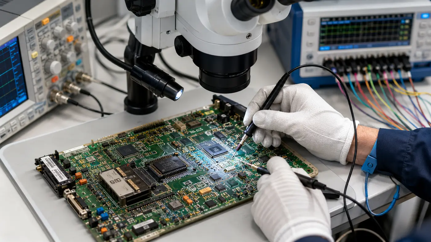
PCB reverse engineering and component identification on an electronics workbench

You can start with a practical problem

You do not need to prepare formal engineering terminology before contacting us. A clear business or equipment problem is enough for an initial technical discussion.

What we do

InspectDocument board revisions, components, connectors and physical construction.
IdentifyResolve component markings and functional roles.
TraceRecover nets, layers and interconnections using suitable methods.
ReconstructCreate schematics and functional block structure.
VerifyCross-check critical circuits against measurements and board behavior.
DocumentPrepare the agreed schematic, BOM and engineering notes.

What the customer receives

The exact deliverable set is agreed before the stage starts so acceptance is based on concrete engineering results rather than activity.

Recovered schematicComponent list/BOMInterface and connector informationFunctional block descriptionInput data for replacement-board development

Technology and implementation

We select the architecture and tools according to interfaces, timing, environment, maintainability and production constraints.

Board inspectionHigh-resolution visual analysis, markings and physical construction.
Net recoveryContinuity, measurements and layer reconstruction where required.
Component identificationPart-number research and functional inference from surrounding circuitry.
MeasurementsPower, signals and protocol behavior when a working sample is available.
DocumentationReadable schematics and engineering notes rather than raw net lists.
Follow-on engineeringModernization, import substitution or compatible-board development.

Electronics and PCB reverse engineering: engineering approach

Reverse engineering is used when the physical device exists but the design documentation is incomplete or unavailable. The depth of reconstruction is selected according to the business goal.

For a certification or maintenance package, the emphasis may be on a clean schematic and BOM. For a replacement project, interfaces, timing and system behavior become equally important.

Multi-layer boards can require destructive layer-by-layer reconstruction. We agree this in advance and define which samples are returnable and which are not.

01

Component identification

02

Net and layer reconstruction

03

Schematic recovery

04

Interface analysis

05

Bench measurements

06

Documentation for redesign

Frequently asked questions

Questions that are useful to settle before the initial estimate.

Do you need a working sample?

A working sample is very useful for measurements, but schematic recovery can also be performed from a non-working board depending on the task.

Can you work with multilayer PCBs?

Yes. Some projects require destructive layer-by-layer analysis; the method and sample use are agreed before work starts.

Do you provide a BOM?

Yes, when component identification is included in the agreed scope.

Can the result be used to make a replacement board?

Yes. Reverse engineering is often the first stage before developing a documented compatible replacement.

Is exact cloning always necessary?

No. In many projects the better goal is to preserve required interfaces and behavior while redesigning the internals on available components.

Discuss your engineering task

Send clear photos of both PCB sides, dimensions, markings, available manuals and a description of what you need to recover.

Useful informationdevice purpose, power, interfaces, operating environment, expected volume, component constraints and target schedule
Customer type