
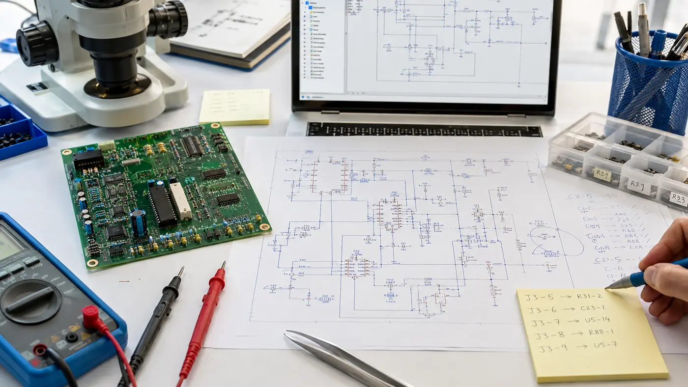
schematic reconstruction

PCB schematic reconstruction from a physical board

We recover readable circuit schematics from assembled printed circuit boards, including component identification, net reconstruction and engineering verification of critical circuits.

Circuit schematic reconstruction from an assembled printed circuit board

You can start with a practical problem

You do not need to prepare formal engineering terminology before contacting us. A clear business or equipment problem is enough for an initial technical discussion.

What we do

PhotographCapture board geometry, markings and assembly details.
IdentifyDetermine component types and values where possible.
TraceRecover electrical connections, including hidden layers when necessary.
DrawRecreate the circuit in logical functional blocks.
CheckVerify critical nets and ambiguous areas by measurement.
ReleaseDeliver schematic and accompanying BOM/notes in the agreed format.

What the customer receives

The exact deliverable set is agreed before the stage starts so acceptance is based on concrete engineering results rather than activity.

Electrical schematicComponent listConnector/pin informationNotes on uncertain or measured valuesSource schematic project when included

Technology and implementation

We select the architecture and tools according to interfaces, timing, environment, maintainability and production constraints.

Visual captureHigh-resolution board documentation before any destructive work.
ConnectivityContinuity and net tracing for accessible circuitry.
Layer analysisLayer-by-layer reconstruction for complex multilayer boards when required.
Component researchMarking and package identification.
Functional groupingPower, processing, interfaces and analog sections organized into readable sheets.
VerificationMeasurement-based checks on critical or ambiguous nodes.

PCB schematic reconstruction from a physical board: engineering approach

A useful recovered schematic must be readable by an engineer. We therefore reorganize physical connectivity into functional sheets and name signals and blocks where their purpose can be established.

The required method depends strongly on layer count, component density and whether destructive analysis of a sample is acceptable.

If the final goal is a new compatible board, schematic reconstruction can be followed by interface analysis, redesign and validation.

01

Board documentation

02

Component identification

03

Connectivity recovery

04

Logical schematic capture

05

Critical-net verification

06

BOM and engineering notes

Frequently asked questions

Questions that are useful to settle before the initial estimate.

Is the board returned?

Non-destructive work can use a returnable sample. Multilayer reconstruction may require a separate non-returnable sample; this is agreed before starting.

Can you recover a four-layer board?

Yes, but hidden layers may require destructive processing depending on density and access.

Is the result suitable for certification documentation?

The schematic and BOM can support documentation work; exact regulatory acceptance requirements should be confirmed for the specific certification process.

Can you identify every component?

Most standard components can be identified, but erased markings, custom parts or damaged devices may require additional analysis or remain documented with uncertainty.

Can you continue with redesign?

Yes. The recovered design can become the starting point for modernization or compatible replacement development.

Discuss your engineering task

Send board photos, layer information if known, dimensions, any available documentation and the required output format.

Useful informationdevice purpose, power, interfaces, operating environment, expected volume, component constraints and target schedule
Customer type